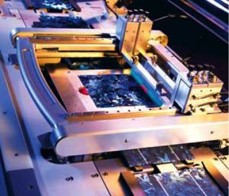
For all the well-deserved hype surrounding advanced solar cell designs, the screen printed (SP) solar cell remains the industry standard. Accounting for approximately 90% of worldwide production in 2014, its robust design has stood the test of time and, since its inception in the 1970s, has ballooned towards current module efficiencies approaching 18%. It has only recently faced serious competition. So why has this design been so successful in fending off competitors?
In short, money talks and it is all due to the ability of SP solar cells to squeeze out as much electricity as possible from relatively low cost materials and processes. The sections below will elaborate on two recent innovations which have continued this trend: advanced screen printing pastes and improved diode engineering.
The Classic Screen Printed Solar Cell Design
The front, light-receiving side of a SP solar cell is typically formed with the three features outlined below.
- Negatively-charged ‘n+ emitter’: the front surface of a typical SP solar cell is ‘doped’ with phosphorus in order to impart an overall negative charge in the silicon material. This negatively charged layer forms one side of the diode needed to create a solar cell – the other positively-charged region of the solar cell is shown in grey in the diagram below. The n+ emitter is incredibly thin. Coming in a less than half a micrometre (µm), it is approximately 100 times thinner than human hair.
- Anti-reflection coating (ARC): The ARC is responsible for reducing the amount of light reflecting off the front surface, as well as improving the electrical properties of the silicon surface. It is an insulating material which restricts the conduction of electricity through it.
- Screen printed silver (Ag) ‘finger’ contacts: The SP silver fingers on the front surface collect electricity generated within the silicon for transport outside of the device, much like the way batteries have metallic terminals on either end. Deposited on top of the ARC as a paste, it must be fired at temperatures of up to 800°C in order to bond the metal particulates and, just as importantly, etch through the ARC in order to allow for electrical contact with the underlying silicon.
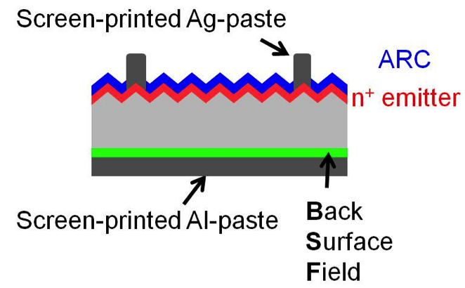
The screen printed silver (Ag) on the front surface must etch through the insulating anti-refection coating (ARC) in order to allow for electrical contact to the underlying silicon solar cell. [Image Source: ISFH]
Although this may appear quite basic, in practice it can be difficult to get right. If the SP paste etches too far through the ARC and ‘eats’ too far into the n+ emitter, there can be severe reductions in cell performance. The trick is to get the metal all the way through the ARC without touching anything but the very top layer of the n+ emitter, which typically contains the highest concentration of phosphorus, allowing for good electrical contact. In general, older SP pastes could not contact more lightly-doped silicon without a subsequent drop in cell performance.
To make matters worse, there is also a limit to how much phosphorus you can put into the front surface of the silicon before it starts to degrade cell performance. In the past, most SP solar cells suffered from a ‘dead layer’ at the front of the device which was caused by having too high a concentration of phosphorus at that region. Unfortunately, it was necessary to have such high emitter doping in order to allow for good electrical contact with the older SP pastes available at the time. For years solar cell manufacturers had produced non-optimal SP cells with a dead layer on the front, largely due to the limitations of the SP paste and emitter formation process.
Screen Printed Paste and Emitter Improvements
All that has changed with two important breakthroughs: (i) SP pastes which can form good electrical contact with lightly-doped silicon; and (ii) emitter formation schemes which reduce dead layer effects. In combination, these two innovations have helped to push SP cell module efficiencies to the levels we see today.
Screen printing paste manufacturers, such as DuPont and Heraeus, have played a large part in these developments. They have producing specialised PV pastes which enable good electrical contact to lightly-doped silicon and etch much less through the emitter during the SP paste firing process. This effectively makes the front metallisation process much more forgiving for solar cell manufacturers.
In addition, the work of researchers in understanding how to reduce the amount of phosphorus doping in the cell – in such a way that the dead layer is effectively eliminated whilst maintaining performance – has also advanced. This design improvement has led to efficiency increases of more than 1% (absolute) for SP cells.
When you consider the gigawatts of solar being produced each year, 1% improvements worldwide accounts for tens of millions of dollars in additional electricity generated. This efficiency boost coming without an increase in manufacturing costs means that we have continued to pay less per watt for our modules.
The humble SP solar cell, despite its unglamorous profile, has and will continue to dominate the PV industry for at least the next decade. But there are challengers waiting in line. In the second part of this series, we will cover one of screen printing’s closest rivals, metal plating. A well-known manufacturing process, it has been a topic of great interest over the past decade, offering the potential to reduce cell metal costs while increasing efficiencies.
© 2015 Solar Choice Pty Ltd
